- 您现在的位置:买卖IC网 > Sheet目录370 > ZXLD1322DCCTC (Diodes Inc)IC LED DRIVR WHITE BCKLGT 14-DFN
A Product Line of
Diodes Incorporated
ZXLD1322
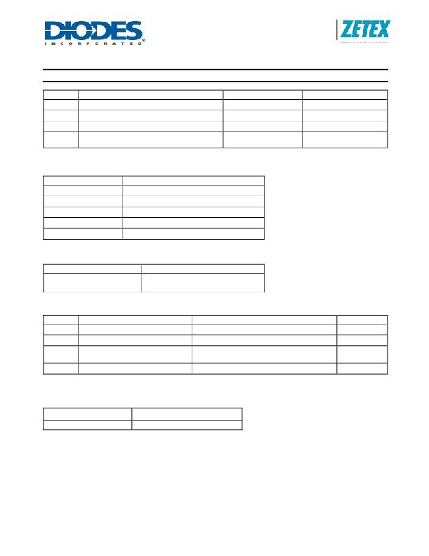
Absolute Maximum Ratings (Voltages to GND Unless Otherwise Stated)
Symbol
T OP
T ST
T J
P TOT
Parameter
Operating Temperature
Storage Temperature
Junction Temperature
Package Power Dissipation
DFN14 with Exposed Pad: 4mm x 3mm, 0.5mm Pitch
Rating
-40 to 125
-55 to 150
-40 to 150
1.5 at T AMB =70°C
Units
°C
°C
°C
W
DC-DC Converter
Supply Voltage (VIN)
ADJ
CFB
I SENSE
T ADJ
BIAS
-0.3V to +15V
-0.3V to The lower of (+5.0V) or (V IN + 0.3V)
-0.3V to The lower of (+5.0V) or (V IN + 0.3V)
-0.3V to The lower of (+5.0V) or (V IN + 0.3V)
-0.3V to The lower of (+5.0V) or (V IN + 0.3V)
-0.3V to The lower of (+5.0V) or (V IN + 0.3V)
High-Side Current Monitor
Monitor Supply Voltage (M_VIN)
Continuous Sense Voltage
(M_V IN – M_LOAD)
Switching NPN Transistor
-0.3V to +15V
-0.3V to +5V
Symbol
V CBO
V CEO
I CM
I C
Parameter
Collector-Base Voltage
Collector-Emitter Voltage
Peak Pulse Current
Continuous Collector Current
Rating
18
18
3
(Pulsed Width = 300μs. Duty Cycle<=2%)
2
Units
V
V
A
A
These are stress ratings only. Operation outside the absolute maximum ratings may cause device failure. Operation at the absolute maximum ratings for
extended periods may reduce device reliability.
Thermal Resistance
Junction to ambient (R θ JC )
DFN4030-14
Nominal Value
26.3°C/W
ZXLD1322
Document number: DS32166 Rev. 3 - 2
4 of 17
www.diodes.com
April 2010
? Diodes Incorporated
发布紧急采购,3分钟左右您将得到回复。
相关PDF资料
ZXLD1350ET5TA
IC LED DRIVR WHITE BCKLGT TSOT-5
ZXLD1352ET5TA
IC LED DRIVER HIGH BRIGHT TSOT-5
ZXLD1356DACTC
IC LED DRIVER WHITE BCKLGT 6-DFN
ZXLD1360ET5TA
IC LED DRIVR WHITE BCKLGT TSOT-5
ZXLD1362ET5TA
IC LED DRIVR WHITE BCKLGT TSOT-5
ZXLD1366DACTC
IC LED DRIVER WHITE BCKLGT 6-DFN
ZXLD1370EST16TC
IC LED DRVR HIGH BRIGHT TSSOP-16
ZXLD1371QESTTC
IC LED DRIVER
相关代理商/技术参数
ZXLD1322DCCTC-CUT TAPE
制造商:DIODES 功能描述:ZXLD1322 Series 15 V 600 kHz 700 mA Buck/Boost Mode DC-DC Converter - DFN-14
ZXLD1322DCTC
制造商:ZETEX 制造商全称:ZETEX 功能描述:Buck/boost mode DC-DC converter for LED driving with 700mA output and current control
ZXLD1350
制造商:ZETEX 制造商全称:ZETEX 功能描述:350mA LED driver with internal switch
ZXLD1350_07
制造商:ZETEX 制造商全称:ZETEX 功能描述:350mA LED driver with internal switch
ZXLD1350ET5
制造商:Diodes Incorporated 功能描述:LED DRIVER INTERNAL SWITCH SMD 制造商:Diodes Incorporated 功能描述:LED DRIVER, INTERNAL SWITCH, SMD 制造商:Diodes Incorporated 功能描述:IC, LED DRIVER, BUCK, TSOT-23-5; Topology:Buck (Step Down); No. of Outputs:1; Output Current:350mA; Output Voltage:30V; Driver Case Style:TSOT-23; Input Voltage Min:7V; Input Voltage Max:30V; Dimming Control Type:PWM / DC ;RoHS Compliant: Yes
ZXLD1350ET5TA
功能描述:LED照明驱动器 7-30V Input 350mA w/Internal Switch RoHS:否 制造商:STMicroelectronics 输入电压:11.5 V to 23 V 工作频率: 最大电源电流:1.7 mA 输出电流: 最大工作温度: 安装风格:SMD/SMT 封装 / 箱体:SO-16N
ZXLD1350ET5TA-CUT TAPE
制造商:DIODES 功能描述:ZXLD1350 Series 350 mA 1 MHz SMT LED Driver with Internal Switch - TSOT-23-5
ZXLD1350EV3
制造商:ZETEX 制造商全称:ZETEX 功能描述:circuit diagram and bill of materials
